DNP Photomask - Milan
Milan, Italy
Project Description
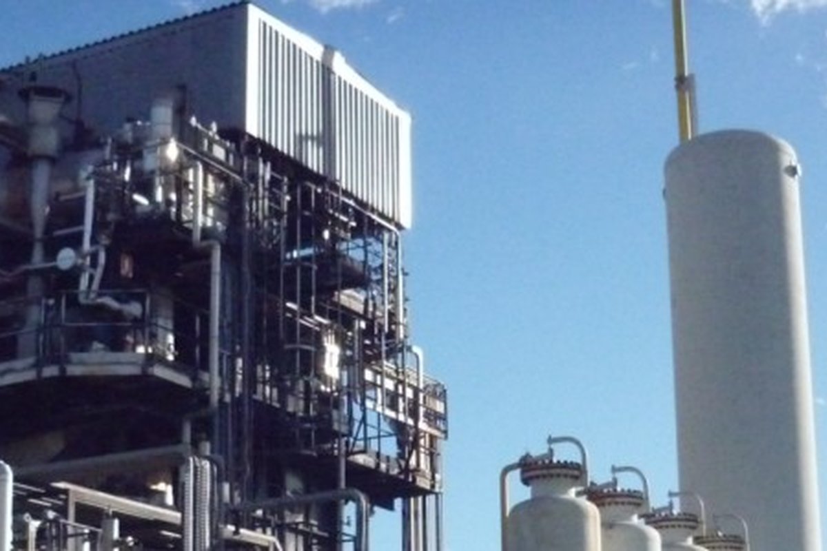
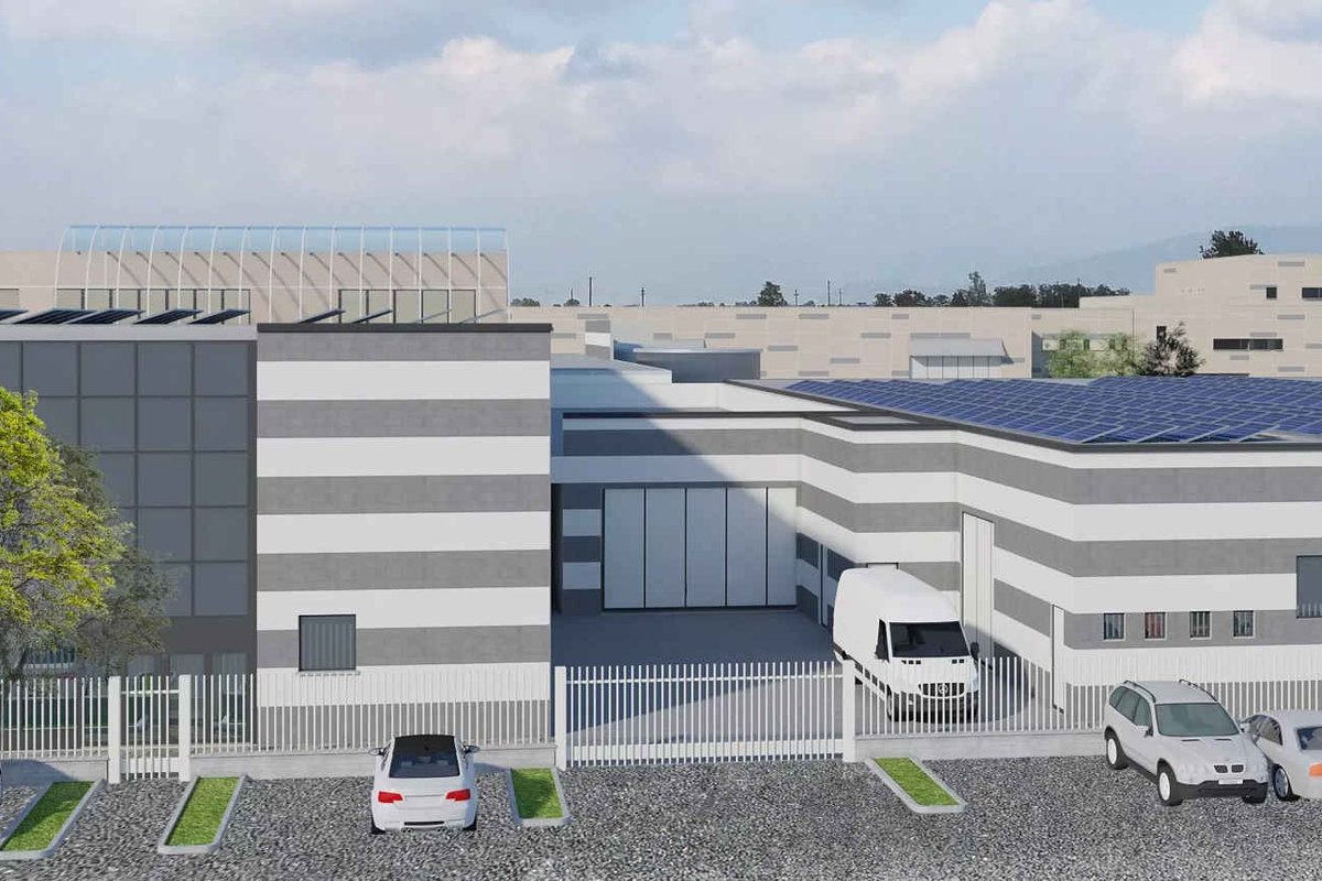
Advanced semiconductor manufacturing facility specializing in photomask production for the electronics industry. TST handled the complete MEP system design and implementation of specialized clean room systems.
This state-of-the-art facility represents cutting-edge technology in semiconductor manufacturing, producing critical components for the global electronics industry.
Main Features
- Total Area: 6,600 m²
- Clean Room Area: 1,250 m²
- Installed Electrical Power: 2,500 kVA
Services Provided by TST
TST provided comprehensive MEP engineering services for this high-tech manufacturing facility, ensuring precision power delivery and specialized systems for semiconductor production.
- Complete MEP system design for clean rooms
- Precision power distribution systems
- Electromagnetic interference (EMI) shielding
- Clean room electrical installations
- Emergency and backup power systems
- Specialized lighting for precision work
- Supply of high-tech electrical equipment
Project Information
Client:
DNP Photomask Europe
DNP Photomask Europe
Year:
2016
2016
Sector:
Semiconductor Manufacturing
Semiconductor Manufacturing
TST Services: